The Scanning Electron Microscope
Enapter has taken a significant step forward in research and development with the commissioning of a state-of-the-art Scanning Electron Microscope (SEM). This advanced tool is crucial for enhancing our AEM electrolyser and serves as the catalyst for our fast and innovative R&D.
13. juillet 2020

Enapter’s commissioning of a cutting edge Scanning Electron Microscope (SEM) is set to push the boundaries of R&D. This powerful piece of equipment is important in advancing Enapter’s AEM electrolyser, especially given the rising demand and the urgency to drive the energy transition. Whether it be batteries, fuel cells, super capacitors or electrolysers, the SEM is the keystone to advancing electrochemical energy storage and conversion systems. It is the linchpin to accelerated R&D of the AEM electrolyser. Here’s why.
SEM meets AEM
Electrochemical systems are at the crossroads of many physical sciences and engineering disciplines, and of particular importance is materials science and how microscale properties affect bulk behaviour. Critical properties governing the performance of electrochemical energy conversion are determined by component surfaces, their interfaces and (sub)micron scale properties of said components.
The same holds true of our Anion Exchange Membrane (AEM) electrolysers. Each and every component of must be tailored at the micron to sub-micron scale to allow for the emergent properties necessary to make the cell and stack excel. Similar to a PEM (Proton Exchange Membrane) in Fuel Cells (PEMFC) and PEM electrolysers, the membrane must be an electronic insulator and an ionic conductor. The main difference is that AEMs conduct anions (i.e. hydroxide, OH–) as opposed to cations (protons, H+). In this way, the AEM is an inherently alkaline environment that allows cheaper, more abundant materials to be utilised. PEM systems, in contrast to an AEM system, require expensive noble metal catalysts made from Iridium, and Titanium components that are stable in highly acidic conditions. AEM electrolysers combine the safety, high current density, and high-pressure benefits of a solid-state ionic conductor, with the abundance and cost effectiveness of classic liquid alkaline electrolysis systems.
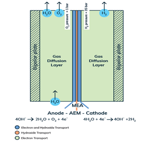
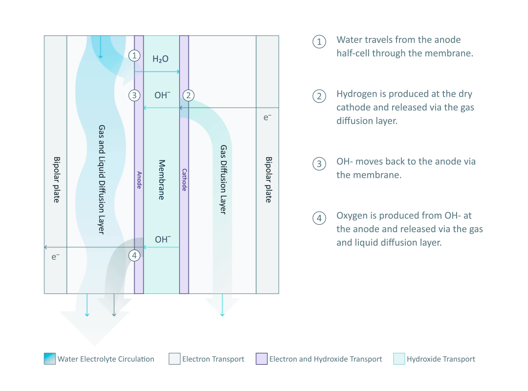
The heart and soul of Enapter’s electrolyser is the AEM stack, which is made of a multitude of single cells. A 2D cross-section of the single cell is shown below, comprised of bipolar plates for electrical current distribution, porous transport layers for proper gas and electrolyte transport, the Anode and Cathode for the Oxygen Evolution Reaction (OER) and Hydrogen Evolution Reaction (HER), respectively, and of course our defining AEM to complete the circuit.
Having to meet halfway between the top-down avenue of engineering with the bottom-up ethos of chemistry and physics is where the SEM is paramount. We’ll discuss how the SEM can be used to unveil important attributes of each component and the effects of nano/micro-scale processes on said components.
Electrolysis reactions
The reactions that define electrolysis, OER and HER, occur on the catalyst layers, which in and of themselves are at the interface between electron and hydroxide conducting media. Both reactions require something called a “triple phase boundary” (TPB) shown in the diagram by Weber et al. Though the diagram is for a PEMFC Anode, the general principle still holds – the reactions we care about only occur at the electron conducting-hydroxide conducting-catalyst particle interface.
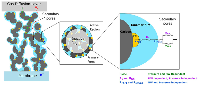
In the context of the PEMFC Anode, the reactant H2 is transported through the void volume (white background) and diffuses to the catalyst particle (Platinum – yellow). The products, protons and electrons, pass through the electron-conducting media of the catalyst layer (Carbon – grey) and the proton-conducting media (Nafion – blue), respectively. To give an order of scale, the blue Nafion thin films and yellow Platinum particles are of the order of 1-10s of nanometers and the grey carbon particles on the micron scale. Secondary Emission (SE) mode on the SEM, having a high resolution, allows us to probe the catalyst layer with distinguishing detail.
To ensure the reaction proceeds, its products must be able to leave the catalyst layer while its reactants are renewed, necessitating the TPB to be maximised. If we look at the OER reaction that occurs at the electrolyser anode, then we must consume hydroxide ions to produce oxygen, electrons and water.
If the TPB is not optimised, then your catalyst utilisation is low. The TPB surface area can be reduced when any of the constituents (catalyst particles, catalyst support, etc.) agglomerate and collapse the catalyst layer, resulting in a reduced triple-phase surface area, reduced porosity, and overall efficiency losses. Further, catalyst particles can potentially disconnect from their supports and relocate in different parts of the cell, reducing cell lifetime. Micron-scale resolution of the catalyst layers as seen with an SEM is critical to illuminating these undesirable phenomena. Used in an end of life analysis after accelerated stress tests, the SEM allows for continuous optimisation and mitigation of these processes under normal operating conditions.
Bipolar plates, porous transport layers and corrosion
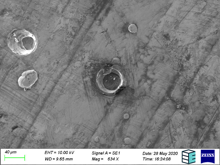
The porous transport layer/gas diffusion layer (PTL/GDL) is a kind of manifold that distributes electrolyte flow into the cell and gases out of the cell. It must have a continuous pore network, allowing for mass transport of gases and electrolyte, while also conducting electrons from the bipolar plate to the catalyst layer. The integrity of such a network can change slowly over time when subjected to thermal and mechanical stresses experienced in normal operating conditions; including the stresses induced on the PTL during stack assembly, thermal cycling during start-up and shutdown, and the potential for the pore network to be clogged by unwanted solid products.
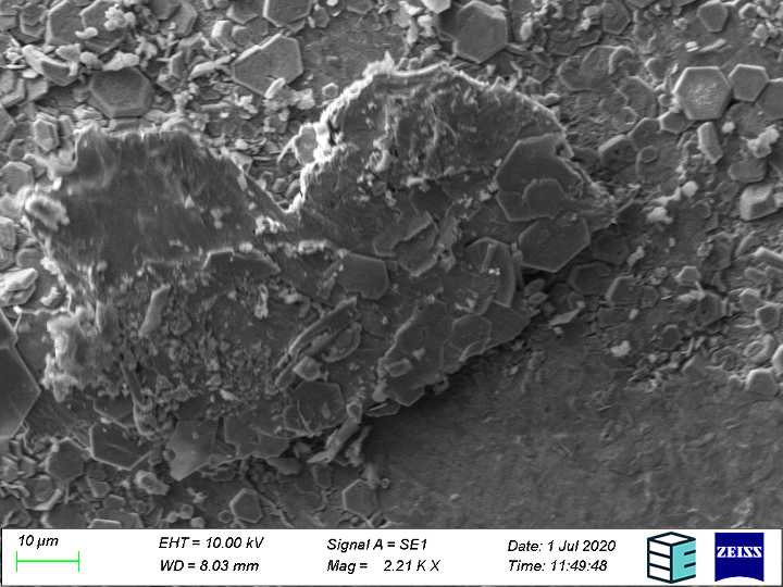
Surface roughening of the electrical current collecting bipolar plates may also occur, with (sub)micron scale insoluble species potentially depositing on other parts of the cell, particularly the PTL’s, and causing runaway efficiency losses. Even though the SEM is only sensitive at and near surfaces, if the cross-section is taken through the plane, the SEM can give a quasi 3D structure (2D+1 if multiple slices are taken). Metallographic cross-sections through the plane of the PTL can be taken at the beginning of life and end of life. Once the sample is prepared, it is brought to an SEM to see how the pore network has changed over time, due to any of the mentioned processes. If the pore networks are collapsed, as would be the case in plastically deformed/overcompressed PTL’s, this would be seen as a sort of “tissue paper” like cross-section.
Further, the bipolar plates can also be imaged to ascertain the type of surface degradation that caused the surface roughening (corrosion, erosion, etc.). The exact mechanism of corrosion can be seen readily at SEM resolutions, as the results from each can be distinguished visually – pitting, crevice, and intergranular corrosion look characteristically different under the SEM.
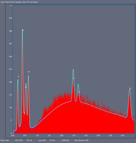
Of crucial interest is the chemical identity of corrosion products to help track their source. Both EDS (Energy Dispersive X-Ray Spectroscopy) and backscattering electron detection can tell you about the chemical elements present in the surface image and their relative abundance, the latter mode being more sensitive to the atomic number (i.e. how “heavy” the atom nucleus is and how far down the periodic table the element is).
Scanning electron microscope interactions
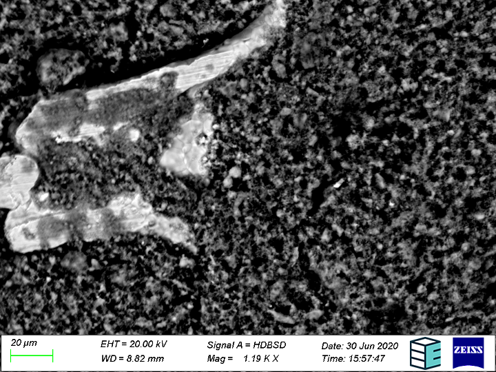
Backscattered electrons – incident electrons elastically “collide” with atoms and bounce back, almost comparatively to hitting a ball. A small amount of kinetic energy of the detected electron is lost, in contrast to an inelastic process. Elastic type collisions occur more frequently with heavier nuclei, such that heavier atoms show up as brighter than lighter atoms, yielding a general chemical element contrast and distribution. As backscattered electrons have very high kinetic energy, detection depth is higher, which in turn lowers the resolution of the surface image as compared to other detectors. Unique chemical identity is not determined with this method, but instead, the relative heaviness of (sub)surface atoms is mapped. This type of detection is crucial when trying to distinguish unique phases, their boundaries, and substrate composition.
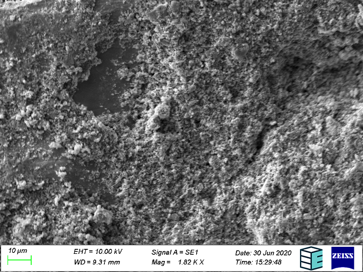
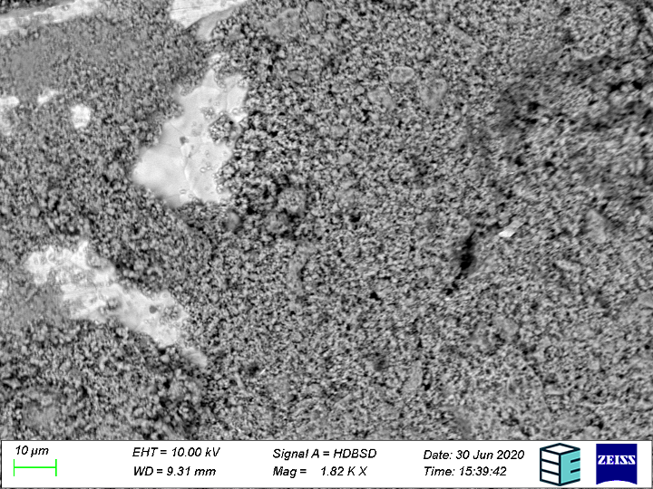
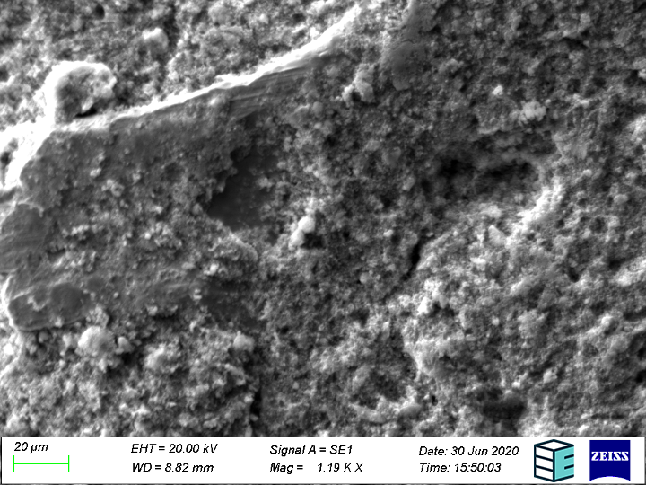
Secondary emission electrons – incident electrons inelastically collide and lose energy as they continue colliding with neighbouring atoms (similar free paths as cosmic particle showers). Secondary electrons are of much lower energy than backscattered electrons, so the detection depth is decreased, allowing nanometer-scale surface resolution. Because of the strong influence of neighbouring atoms, surfaces can be highly detailed as shown below – containing rich mountains and valleys revealing that the smoothest of surfaces have inherent roughness. Topological information gained from this type of detection is essential for corrosion and surface roughness studies.
The images below show the same region of a substrate under the two modes of operation discussed so far: secondary emission and backscattering detection. In this case, backscattering shows phase separations and relative density in detail. In secondary emission mode, surface details are more defined, but phase separations are not.
Energy Dispersive X-ray Spectroscopy (EDS/EDX) – an added type of interaction that diverts from the classical elastic/inelastic picture includes the possibility of electrons causing substrate atom electrons to eject, leave “electron holes”, and be subsequently refilled (or cause more substrate electron ejections, i.e. auger electrons). If an electron which is occupying a higher energy orbital drops in energy to fill a hole in a lower level, the atom releases a photon of the same energy as between the two orbitals; in this case an X-ray photon. Due to the unique electronic structure of every element in the periodic table, atomic X-ray emissions are also unique, yielding elemental “fingerprints”. This technique, coupled with a backscattering detector, allows for a full elemental mapping of a surface for most elements heavier than Beryllium. This method, when combined with backscattering and secondary emission detection data, gives us a full map of elemental composition and relative abundance on an imaged sample.
With all three modes of operation used, failure mechanisms can be analysed, classified, and mitigated in future components. This powerful characterisation is why the SEM is used in so many industries, especially battery and automotive. The processes that limit lifetime, such as corrosion, mechanical fatigue, start on the microscale. By the time they become visible to the naked eye, the damage is irreversible and safety becomes a concern.
In order to make an electrolyser that lasts as long as possible, with negligible efficiency losses over its lifetime, the SEM must be used to facilitate R&D, perform post failure analysis, and ensure quality control of each component used.
A cut above the rest
The SEM is undeniably a vital tool for research in a science dominated by surfaces and their interfaces. It helps streamline processes in many ways while making trials incredibly effective. The commission of such an incredible device like the SEM is set to make critically important parameters that were previously unknown, known.
For further insights read more about AEM Electrolysis technology or contact our team to get started with your own green hydrogen project soon.
by Enapter Chemistry Team
Thanks for reading, and feel free to share this with anyone you think would appreciate it.